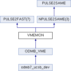
module that monitors various registers, sets certain voltaile settings, and sends reset signals
More...
|
|
SLOWCLK | in |
| | 2.5 MHz clock.
|
|
CLK40 | in |
| | 40 MHz clock. Used for resets and pulses.
|
|
RST | in |
| | Firmware soft reset signal.
|
|
DEVICE | in |
| | Indicates if this is the selected ODMB VME device.
|
|
STROBE | in |
| | Strobe signal indicating VME command is ready.
|
|
COMMAND | in ( 9 downto 0 ) |
| | VME command signal.
|
|
WRITER | in |
| | Indicates if VME command is a read or write command.
|
|
INDATA | in ( 15 downto 0 ) |
| | Input data accompanying VME command.
|
|
OUTDATA | out ( 15 downto 0 ) |
| | Output data to VME backplane.
|
|
DTACK | out |
| | Data acknowledge, indicates the VME command has been received.
|
|
DCFEB_DONE | in ( NCFEB downto 1 ) |
| | DCFEB done bits.
|
|
OPT_RESET_PULSE | out |
| | Signal to reset optical firmware.
|
|
L1A_RESET_PULSE | out |
| | Signal to reset L1A counter.
|
|
FW_RESET | out |
| | ODMB firmware soft reset signal.
|
|
REPROG_B | out |
| | REPROGRAM signal to (x)DCFEBs.
|
|
TEST_INJ | out |
| | Signal to generate test INJPLS to (x)DCFEBs.
|
|
TEST_PLS | out |
| | Signal to generate test EXTPLS to (x)DCFEBs.
|
|
TEST_LCT | out |
| | Signal to generate test LCTs to (x)DCFEBs.
|
|
TEST_BC0 | out |
| | Signal to generate test BC0 to (x)DCFEBs.
|
|
OTMB_LCT_RQST | out |
| | LCT request signal to OTMB.
|
|
OTMB_EXT_TRIG | out |
| | External trigger request signal to OTMB.
|
|
ODMB_CAL | out |
| | Sets calibration mode (L1A generated with INJPLS) in TRGCTRL.
|
|
TP_SEL | out ( 15 downto 0 ) |
| | Test point select signal.
|
|
MAX_WORDS_DCFEB | out ( 15 downto 0 ) |
| | Maximum number of words before an (x)DCFEB is marked as bad.
|
|
LOOPBACK | out ( 2 downto 0 ) |
| | For internal loopback tests, currently unused.
|
|
TXDIFFCTRL | out ( 3 downto 0 ) |
| | Controls the TX voltage swing, currently unused.
|
|
MUX_DATA_PATH | out |
| | Controls whether data comes from real boards or simulated data.
|
|
MUX_TRIGGER | out |
| | Controls whether trigger signals are external or come from TESTCTRL.
|
|
MUX_LVMB | out |
| | Controls whether LVMB communication is to real board or simulated LVMB.
|
|
ODMB_PED | out ( 1 downto 0 ) |
| | Controls pedestal (genereates L1A MATCH for each L1A)
|
|
TEST_PED | out |
| | Control whether OTMB data is requested for each L1A.
|
|
MASK_L1A | out ( NCFEB downto 0 ) |
| | Suppresses L1A and L1A_MATCHes.
|
|
MASK_PLS | out |
| | Suppresses INJPLS and EXTPLS signals.
|
|
ODMB_DATA_SEL | out ( 7 downto 0 ) |
| | Selects top level data signal to read.
|
|
ODMB_DATA | in ( 15 downto 0 ) |
| | Data from top level.
|
module that monitors various registers, sets certain voltaile settings, and sends reset signals
Supported VME commands:
- W/R 3000 write or read ODMB calibration mode. 0=nominal mode, 1=calibration mode (L1A with each pulse)
- W 3004 ODMB firmware soft reset
- W 3008 ODMB optical reset
- W 3010 DCFEB reprogram (hard reset)
- W 3014 L1A reset and DCFEB resync
- W/R 3020 write or read test point select
- W/R 3024 write or read the maximum number of bad words from (x)DCFEB before they are killed
- W/R 3100 write or read loopback setting. 0=no loopback, 1 or 2=internal loopback
- R 3110 read TX voltage swing. 0=minimum (100 mV), F=maximum (1100 mV)
- R 3120 read (x)DCFEB programming done bits
- w 3200 generate pulses. bits: 0=INJPLS, 1=EXTPLS, 2=L1A+L1A_MATCH, 3=LCT request to OTMB, 4=external trigger request to OTMB, 5=BC0
- W/R 3300 write or read data multiplexer. 0=real data, 1=dummy data.
- W/R 3304 write or read trigger multiplexer. 0=external triggers, 1=internal triggers.
- W/R 3308 write or read LVMB multiplexer. 0=real LVMB, 1=dummy LVMB.
- W/R 3400 write or read pedestal (L1A_MATCH for each L1A). 0=normal, 1=pedestal.
- W/R 3404 write or read. 0=normal, 1=OTMB data requested for each L1A.
- W/R 3408 write or read L1A mask. bit 0=kills L1A, bits 1-7=kills L1A_MATCHes
- W/R 340C write or read mask_pls. 0=normal, 1=no EXTPLS/INJPLS
- R 3YZC read data registers. YZ determines the data to be read, see top level.
The documentation for this class was generated from the following file:
- /homes/oshiro/odmb/firmware/odmb7_ucsb_dev/source/odmb_vme/vmemon.vhd

 1.8.5
1.8.5