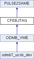
module handling JTAG (slow control) communication to (x)DCFEBs within ODMB VME
More...
|
|
FASTCLK | in |
| | 40 MHz clock. Currently unused.
|
|
SLOWCLK | in |
| | 1.25MHz clock (previously 2.5 MHz clock, but this was too fast for some HD50 cables)
|
|
RST | in |
| | Firmware soft reset signal.
|
|
DEVICE | in |
| | Indicates if this is the selected ODMB VME device.
|
|
STROBE | in |
| | Strobe signal indicating a VME command is ready.
|
|
COMMAND | in ( 9 downto 0 ) |
| | VME command signal.
|
|
WRITER | in |
| | Indicates if VME command is a read or write command. Currently unused.
|
|
INDATA | in ( 15 downto 0 ) |
| | Input data accompanying VME command.
|
|
OUTDATA | out ( 15 downto 0 ) |
| | Output data to VME backplane.
|
|
DTACK | out |
| | Data acknowledge, indicates that VME command has been received.
|
|
INITJTAGS | in |
| | Signal generated when (x)DCFEBs finish programming to invoke a reset of the JTAG state machine.
|
|
TCK | out ( NCFEB downto 1 ) |
| | JTAG test clock signal to (x)DCFEBs. One per (x)DCFEB to allow communication with a single board.
|
|
TDI | out |
| | JTAG test data in signal to (x)DCFEBs.
|
|
TMS | out |
| | JTAG test mode select signal to (x)DCFEBs.
|
|
FEBTDO | in ( NCFEB downto 1 ) |
| | JTAG test data out signal from (x)DCFEBs.
|
|
LED | out |
| | Debug signals.
|
|
DIAGOUT | out ( 17 downto 0 ) |
| | Debug signals.
|
module handling JTAG (slow control) communication to (x)DCFEBs within ODMB VME
Supported VME commands:
- W 1Y00 shift Y+1 data bits with no JTAG header or tailer
- W 1Y04 shift Y+1 data bits with JTAG header
- W 1Y08 shift Y+1 data bits with JTAG tailer
- W 1Y0C shift Y+1 data bits with JTAG header and tailer
- R 1014 read last data bits shifted into TDO register
- W 1018 send JTAG reset pattern
- W 1Y1C identical to W 1Y3C
- W 1020 select (x)DCFEBs; one bit per (x)DCFEB
- R 1024 read selected (x)DCFEBs
- W 1Y30 shift Y+1 instruction bits with no JTAG header or tailer
- W 1Y34 shift Y+1 instruction bits with JTAG header
- W 1Y38 shift Y+1 instruction bits with JTAG tailer
- W 1Y3C shift Y+1 instruction bits with JTAG header and tailer
- W 1Y48 shift Y+1 instruction bits with special JTAG tailer
- W 1Y4C shift Y+1 instruction bits with JTAG header and special JTAG tailer
The documentation for this class was generated from the following file:
- /homes/oshiro/odmb/firmware/odmb7_ucsb_dev/source/odmb_vme/cfebjtag.vhd

 1.8.5
1.8.5