The frequency response of the simple circuit given by SPICE is plotted
with the measured data of strip 120 on the p-side of the 1B3 part with
full bias voltage of 40V as shown Fig. 3. The
simulation does not match well with the data. However, we can see the
important features of the model. The initial downward slope is due to
![]() . When the magnitude of the impedance of
. When the magnitude of the impedance of ![]() given by
given by
![]() equals
equals ![]() , the bias resistor begins to dominate
and we see the flat region. When
, the bias resistor begins to dominate
and we see the flat region. When ![]() equals
equals
![]() , then
the impedance starts to turn downwards again. At very high
frequencies beyond 1 MHz and off the plot, we see another flat region
where
, then
the impedance starts to turn downwards again. At very high
frequencies beyond 1 MHz and off the plot, we see another flat region
where ![]() dominates. A few things to note about the plot are that
there is some sort of interference, perhaps a radio station, at 800kHz
and 250kHz and possibly the regions around those frequencies.
dominates. A few things to note about the plot are that
there is some sort of interference, perhaps a radio station, at 800kHz
and 250kHz and possibly the regions around those frequencies.
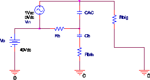
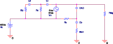
At this point, there are two things that we can do. The first is to assume that the parasitic elements due to the probe station is in parallel with the model and try to extract the data that is just the detector. The assumption that the parasitics are in parallel with the detector is a bad one at higher frequencies when the interstrip capacitances come into effect and we no longer have a parallel model. The second thing to try is to model the raw data by adding parasitic elements to the simple SPICE model that we have. Of course none of this has taken into account the adjacent strips yet.
First, we will take a look at modeling the raw data by adding extra
elements into the original simple model. We put a capacitor in series
with an element consisting of a resistor in parallel with a series RC
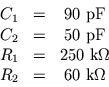
(see Fig. 4). The values of ![]() ,
, ![]() ,
, ![]() , and
, and
![]() are arbitrary and chosen to fit the data (see
Fig. 5). It is not known at this point whether
this model is meaningful in any way, and it fails at high frequencies.
The values for the
are arbitrary and chosen to fit the data (see
Fig. 5). It is not known at this point whether
this model is meaningful in any way, and it fails at high frequencies.
The values for the
 |
(4) |
 |
(5) |
Now we take a look at a circuit that only includes the parasitic part
(see Fig. 7). This SPICE model is compared with the data
of a plucked strip 108 on the p-side of the 1B3 part at 40V bias (see
Fig. 8 and 9). From this, we can
see if the model of the parasitic elements matches the data on a
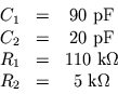
plucked strip. The first plot is for the first set of values for
![]() ,
, ![]() ,
, ![]() , and
, and ![]() and the second plot is for the second
set of values listed above.
and the second plot is for the second
set of values listed above.
The second thing to try is to assume that the parasitic element is in
parallel with what is being measured. Let ![]() be the total
impedance of a normal strip. If we measure the impedance
be the total
impedance of a normal strip. If we measure the impedance ![]() of a
strip that is plucked between the upilex and the wafers, then we can
subtract out the effect of
of a
strip that is plucked between the upilex and the wafers, then we can
subtract out the effect of ![]() , the parasitics due to the probe and
possibly the upilex. What we are then left with is
, the parasitics due to the probe and
possibly the upilex. What we are then left with is ![]() , the
impedance of the silicon detector. The extraction process works as
follows. The total impedance is given by
, the
impedance of the silicon detector. The extraction process works as
follows. The total impedance is given by
| (6) |
| (7) | |||
| (8) | |||
| (9) |
| (10) |
| (11) |
| (12) |
Now we can attempt to plot the data given by SPICE for the simple
model (see Fig. 2), against this newly extracted data.
The plots are shown in Fig. 10. We can
see that at low frequencies, the extraction process works well.
However, when the neighboring strips become important and ![]() comes into play, we get a deviation from the model.
comes into play, we get a deviation from the model.
To go even further, we can add the neighboring strips into the model,
as well as break up the strip itself into a series of capacitors and
resistors. We put in the interstrip capacitances and in addition, we
put in an implant resistance ![]() , which has a value of about 54
k
, which has a value of about 54
k![]() /cm which gives about
/cm which gives about
![]() , and a upilex
interstrip capacitance
, and a upilex
interstrip capacitance ![]() which is about 0.5 pF/cm giving a value
of about 3pF.
which is about 0.5 pF/cm giving a value
of about 3pF.
At this point, we need to get into the details of how the probe works. The probe has 256 pins. 252 of them are all connected together and float. Of the four remaining, one is the test strip and the other three are floating. The test strip is always next to one floating strip on one side and two floating strips on the other side.
The only way to get anything close to the measured data is to include
the parasitic elements shown previously in Fig. 7. We
find that the impedance and phase no longer change after adding about
48 neighboring strips. We also find no change after dividing the
strip up into four segments, each with their own interstrip and AC
coupling capacitances. In this model, we have to alter the values
that we used previously for ![]() ,
, ![]() ,
, ![]() , and
, and ![]() to get a
good fit of the data. Also, a different value of
to get a
good fit of the data. Also, a different value of ![]() was used other
than 3pF. This might have to do with the fact that there is also an
interstrip capacitance between upilex strips that are 2 apart in
addition to the nearest neighbor interstrip capacitance.
Additionally, the value of
was used other
than 3pF. This might have to do with the fact that there is also an
interstrip capacitance between upilex strips that are 2 apart in
addition to the nearest neighbor interstrip capacitance.
Additionally, the value of ![]() is important at very low
frequencies.
is important at very low
frequencies. ![]() actually represents the leakage to the backplane
and to get a better fit around 50 Hz, we set that value as well. The
values used to produce the plot in Fig. 11 are
actually represents the leakage to the backplane
and to get a better fit around 50 Hz, we set that value as well. The
values used to produce the plot in Fig. 11 are
 |
(13) |
Another parameter that we can vary is the bias voltage ![]() . As the
bias voltage drops, the capacitance to the backplane should increase
as the charge carriers get closer to each other and the depletion
region shrinks. The capacitance
. As the
bias voltage drops, the capacitance to the backplane should increase
as the charge carriers get closer to each other and the depletion
region shrinks. The capacitance ![]() should be proportional to
should be proportional to
![]() . The question is if this effect can be seen, and if we
can quantitatively extract the value of
. The question is if this effect can be seen, and if we
can quantitatively extract the value of ![]() by taking measurements.
One thing to be careful of is the amplitude of the input frequency.
If it is comparable to the bias voltage, then we could see unwanted
effects. So for this data, the bias voltage was at 100 mV. Because
of noise, we begin taking data at 200 Hz rather than 20 Hz. We expect
that
by taking measurements.
One thing to be careful of is the amplitude of the input frequency.
If it is comparable to the bias voltage, then we could see unwanted
effects. So for this data, the bias voltage was at 100 mV. Because
of noise, we begin taking data at 200 Hz rather than 20 Hz. We expect
that ![]() affects only higher frequencies and so this shouldn't be a
problem. Fig. 12 is a plot of the impedance and phase at
various bias voltages.
affects only higher frequencies and so this shouldn't be a
problem. Fig. 12 is a plot of the impedance and phase at
various bias voltages.
![\includegraphics[width=2.5in]{simple_imp}](img20.png)
![\includegraphics[width=2.5in]{simple_phase}](img21.png)
![\includegraphics[width=2.5in]{parasitic_imp1}](img29.png)
![\includegraphics[width=2.5in]{parasitic_phase1}](img30.png)
![\includegraphics[width=2.5in]{parasitic_imp2}](img31.png)
![\includegraphics[width=2.5in]{parasitic_phase2}](img32.png)
![\includegraphics[width=2in]{plucked}](img33.png)
![\includegraphics[width=2.5in]{plucked_imp1}](img34.png)
![\includegraphics[width=2.5in]{plucked_phase1}](img35.png)
![\includegraphics[width=2.5in]{plucked_imp2}](img36.png)
![\includegraphics[width=2.5in]{plucked_phase2}](img37.png)
![\includegraphics[width=2.5in]{extracted_imp}](img53.png)
![\includegraphics[width=2.5in]{extracted_phase}](img54.png)
![\includegraphics[width=2.5in]{model_imp}](img60.png)
![\includegraphics[width=2.5in]{model_phase}](img61.png)
![\includegraphics[width=2.5in]{bias_imp}](img64.png)
![\includegraphics[width=2.5in]{bias_phase}](img65.png)
![\includegraphics[width=2.5in]{bias_imp_1k}](img69.png)
![\includegraphics[width=2.5in]{bias_phase_1k}](img70.png)
![\includegraphics[width=2.5in]{bias_imp_10k}](img71.png)
![\includegraphics[width=2.5in]{bias_phase_10k}](img72.png)
![\includegraphics[width=2.5in]{bias_imp_100k}](img73.png)
![\includegraphics[width=2.5in]{bias_phase_100k}](img74.png)
![\includegraphics[width=2.5in]{bias_Z2_1k}](img75.png)
![\includegraphics[width=2.5in]{bias_Z2_10k}](img76.png)
![\includegraphics[width=2.5in]{bias_Z2_100k}](img77.png)