


Next: 4 The Probe Station
Up: Frequency Response Properties of
Previous: 2 p-side of the
Contents
We now switch to the n-side of the detector. Many of the measurements
at a bias voltage of 40V are very similar to those of the p-side.
This may be an indication that the parasitic elements in the probe
dominate over anything we are trying to see in the detector itself.
The n-side is different in several ways from the p-side. There are
two wafers whose strips run along the length of the detector, compared
to the p-side where the strips run along the width of the detector.
The AC metal strips above are connected together and while each strip
still has its own bias resistor. This means that when we measure the
impedance between the AC metal and the bias line, we measure twice the
 since there are two strips connected together. In addition,
we also see two
since there are two strips connected together. In addition,
we also see two  in parallel and so the resistance appears to be
half that of the bias resistance. We show some data for an n-side
strip 252 at 1V input amplitude and full bias of 40V along with the
data from the p-side for comparison in Fig. 15.
in parallel and so the resistance appears to be
half that of the bias resistance. We show some data for an n-side
strip 252 at 1V input amplitude and full bias of 40V along with the
data from the p-side for comparison in Fig. 15.
Figure 15:
Impedance and phase measurements for both sides
|
|
From the plots, it can be seen that the most difference is found at
low frequencies where the value of the bias resistance is effectively
halved compared to the p-side. The value for is about 96 pF
for n-side, however, the probe at low frequencies effectively see
twice that amount so that the effective value is 192pF which is about
the same as on the p-side.
We can do the same type of modeling for the n-side with a network of
resistors and capacitors. If we assume that the parasitics are the
same, meaning that we keep the values that we used for the p-side,
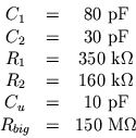 |
(14) |
we get somewhat good agreement as show in Fig. 16.
Figure 16:
Simulation of a complicated network model vs. data
|
|
By altering some of the values shown above, we can get better
agreement as shown in Fig. 17 using the values
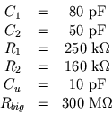 |
(15) |
Figure 17:
Simulation of a complicated network model vs. data
|
|
Another distinction between the n-side and the p-side is that the
n-side has p-doped p-stops between the strips to prevent them from
shorting together. The p-stops only work when the detector is fully
depleted, which happens at around 30V. So as we vary the bias voltage
on the n-side, the strips start shorting together and so we should see
effectively more and more resistors in parallel. So the effective
value of should drop and we can see this clearly from the plots
shown in Fig. 18.
Figure 18:
Impedance and phase at various bias voltages
|
|
Next: 4 The Probe Station
Up: Frequency Response Properties of
Previous: 2 p-side of the
Contents
![\includegraphics[width=2.5in]{nside_imp}](img78.png)
![\includegraphics[width=2.5in]{nside_phase}](img79.png)
![\includegraphics[width=2.5in]{nside_model_imp}](img80.png)
![\includegraphics[width=2.5in]{nside_model_phase}](img81.png)
![\includegraphics[width=2.5in]{nside_model_imp2}](img83.png)
![\includegraphics[width=2.5in]{nside_model_phase2}](img84.png)
![\includegraphics[width=2.5in]{nside_bias_imp}](img85.png)
![\includegraphics[width=2.5in]{nside_bias_phase}](img86.png)