Next: 2 p-side of the
Up: Frequency Response Properties of
Previous: Contents
Contents
We attempt to model the frequency response of the silicon vertex
detector for BaBar with a network of capacitors and resistors using
PSPICE and compare to measurements. Specifically we measure the
impedances and phases of a 1B3 part which is a Layer 1 backward part.
The important capacitances and resistances are the capacitances
between the AC metal strip and the implant  , the bias
resistance
, the bias
resistance  , the bulk capacitance from one strip to a single
strip on the backplane
, the bulk capacitance from one strip to a single
strip on the backplane  , and the interstrip capacitance
between implants
, and the interstrip capacitance
between implants  . In addition, each strip also sees an
effective resistance to ground after going through to
the backplane. If
. In addition, each strip also sees an
effective resistance to ground after going through to
the backplane. If  is the number of strips, then each strip sees
capacitors and resistors in series (see
Fig. 1). The equivalent circuit for this is a single
capacitor with value
is the number of strips, then each strip sees
capacitors and resistors in series (see
Fig. 1). The equivalent circuit for this is a single
capacitor with value  in series with a resistor with
value
in series with a resistor with
value  . From now on, we will define
 while still referring to the resistance as .
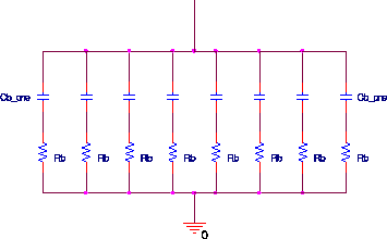
Figure 1:
The capacitances and resistances to the backplane, which can be
simplified to a single resistance and capacitance
|
|
We study the frequency response of the detector with an LCR probe
between the AC metal strip and the implant for frequencies between
about 10 Hz and 1 MHz with an amplitude of 1V for the input frequency.
For actual measurements, there are many parasitic elements between the
probe and the detectors, such as those of the relay boards. We will
see that the data does not agree very well with the SPICE simulations,
although there are some ways of compensating for the parasitic
elements.
The values we use for the detector are
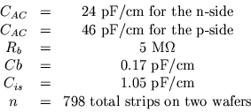 |
(1) |
Each wafer is 4 cm by 4 cm and there are two wafers placed side by
side. On the p-side, there are strips on each wafer running along
the short side. On the n-side, the strips run along the long side and
so there are strips on each wafer that are linked by AC metal
strips that are connected between wafers. Both sides still end up
seeing  and
and  to the backplane assuming that the interaction
between strips on different wafers is negligible. So on each side, we
multiply by 4cm to get the total values. The values we get for the
p-side are
to the backplane assuming that the interaction
between strips on different wafers is negligible. So on each side, we
multiply by 4cm to get the total values. The values we get for the
p-side are
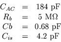 |
(2) |
while the values for the n-side are
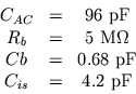 |
(3) |
Next: 2 p-side of the
Up: Frequency Response Properties of
Previous: Contents
Contents