SVT Gains and Offsets from UCSB TestBench
This document summarizes the procedure used to extract electronics
gains, offsets and noise on a Type-B layer 2 module with a hybrid fully
loaded (7 chips/side) with first version radiation-soft chips.
- All measurements were performed with 100 nsec shaping time.
- The clock frequency was 40 MHZ.
- We used the prototype wire-wrap DAQ-link and HDI-link cards, with
transistor-based level shifting. We used the prototype
wire-wrap matching card for the earlier measurements on the unbonded
hybrid.
For the measurements on the bonded detector,
we switched to the PC version of the matching card.
- The hybrid and the matching card were connected through a
a set of two short single layer flat kapton circuits
and a home-made cable harness.
In this harness, digital signals were transmitted on 50 ohm coaxial
cables with their shield tied to digital ground.
- Power was supplied by a set of benchtop power supplies.
Voltage levels were set at the beginning of each run using the sense
lines brought out from the HDI.
Currents on
the 5V and 2V supplies to the hybrid were monitored with digital multimeters
in series with the power lines. Silicon currents were monitored
using nanoammeters.
- Gains, offsets, and noise were measured with the
detector in the ring frame. A noise measurement was repeated
after attachment of the ribs, with the detector in the test-beam box
using tails provided by the INFN-Milano group. This test yielded
consistent results. Noise measurements were also made using
the new version of the data transmission system with the module in
the test-beam box. Initially, these measurement showed one order
of magnitude higher noise levels. After some reconfiguring of cabling etc.,
the noise as measured with the new data transmission was reduced
and was found to be comparable to the noise measured with the old
data transmission system (although still worse by 10% or so).
- Gains Offsets and Noise
- Measurements of gains and offsets
were based on a series of threshold
scans at fixed charge injection (with different charge injection
values for different runs).
- The charge injection circuitry was fired for only one channel per
chip at a time.
- Typically, for each threshold and charge injection setting, each
channel was fired 50 times.
- The 50% firing point and the noise for each channel
were extracted from a fit
of the threshold turn-on curves to an error function using binomial
errors and constraining the top of the threshold curve to
100% efficiency. Two typical fits for bonded channels
are shown in Figure 1. (Postscript
version of Figure 1).
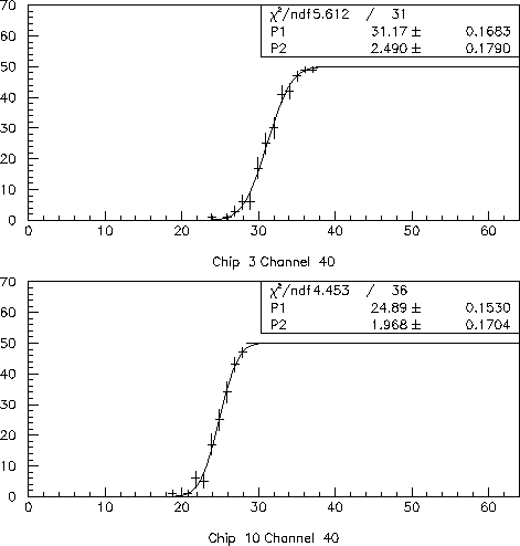
Figure 1: Results of threshold scans at fixed charge
injection for
a bonded channel on the n- (phi-) side (Chip 3,
Channel 40) and a bonded channel on
the p- (z-) side (Chip 10 Channel 40).
What is plotted is the number of firings as a function of threshold
measured in Threshold DAC counts.
Note that here threshold decreases left-to-right.
The fit parameters P1 and P2 in Figure 1
give the 50% turn on
point and the gaussian noise component in Threshold DAC counts
respectively.
As we will describe below,
one Threshold DAC count corresponds to
a charge of approximately 400 electrons.
- The gains and offsets were then extracted by fitting the 50%
firing points for each channel as a function of different charge
injection settings. The fits to extract gains and offsets for
the same two channels of Figure 1, are shown in Figure 2.
(Postscript
version of Figure 2).
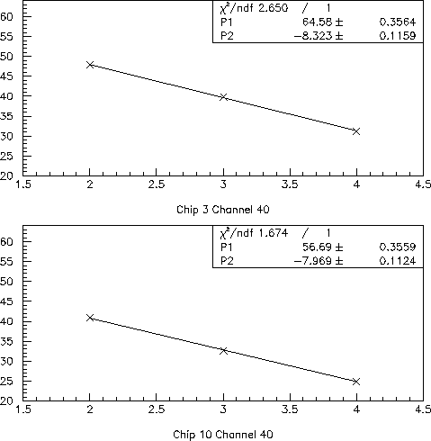
Figure 2: Linearity fits for
a bonded channel on the n- (phi-) side (Chip 3,
Channel 40) and a bonded channel on the p- (z-) side
(Chip 10 Channel 40). On the horizontal axis we plot the value of the injected
charge, in units of Calibration DAC counts; on the vertical axis we plot
the 50% turn on point, in unit of Threshold DAC counts.
The fit parameters P1 and P2 in Figure 2 give, respectively,
offset and gain in units of DAC counts. Note that with this convention,
a channel with zero offset (in mV) would have an offset of 63 Threshold
DAC counts.
- To convert from
Threshold DAC and Calibration DAC counts to
SI units, we used the following factors:
- Threshold DAC: 4.29 mV/count
- Calibration DAC: 8.217 mV/count
- Charge injecting capacitor: 65 fF
- Using the above values, Calibration DAC: 65*0.008217=0.51 fC/count
- The gain and offset variations for two chips bonded to the
detector are shown in Figure 3 (Postscript
version of Figure 3).
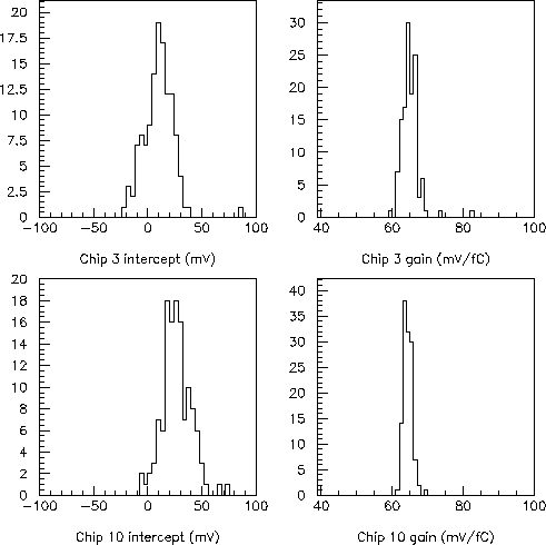
Figure 3: Gains and offsets for chip 3 (n- or
phi-side) and chip 10 (p- or
z-side)
- The noise for all channels in the module for a typical run is
shown in Figure 4 (Postscript
version of Figure 4).
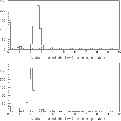
Figure 4: Noise in Threshold DAC counts for all channels
on the n- (phi-) and p- (z-) sides
of the detector as measured in a typical threshoold scan.
To convert the noise measurement from Threshold DAC counts to number of
electrons, we use the conversion factors given
above, and a typical gain
of 65 mV/fC (see Figure 3):
Thus, the typical noise seen is approximately
- ~ 2.6 Threshold DAC counts = 1070 electrons
on the n- (phi-) side
- ~ 2.1 Threshold DAC counts = 860 electrons
on the p- (z-) side
which can be compared with the latest predictions of Issy Kipnis'
simulation for a Layer 2 detector:
- ~ 810 electrons
on the n- (phi-) side
- ~ 660 electrons
on the p- (z-) side
All channels on the module are included in the plots of Figure 4, i.e.
known bad channels and unbonded channels have not been removed.
The pileup of channels at zero noise is due to dead channels. One of the
seven chips on the n-side of the detector is effectively dead,
since both channel and calibration masks appear to be stuck in an OFF
state. The other clump of channels with noise of order 0.8 Threshold
DAC counts is due to unbonded channels. Note also that some of the
spread in the noise values is due to the statistical uncertainty on
the noise measurement, which is typically of order 0.2 Threshold DAC
counts (see the fits in Figure 1):
- Channel-by-channel gains, offsets, and noise are tabulated in the
EXCEL spread sheet which contains also the bonding map and the
list of bad channels. This spread sheet is available through
a link from the UCSB test-beam page.
More plots/information is also available on
request.
![[TestBeam] border=](../hf/Rarrow02.gif) Return to UCSB test-beam page
Return to UCSB test-beam page
Claudio Campagnari &
Doug Roberts