Go To : [Introduction] [Pictures]
[Electronics Measurements] [Operational
hints] [Bonding Map]
Last Updated: May 7, 1997
We have constructed a Layer 2 Module for use in the May '97 SVT Test Beam at CERN. This module consists of one backward Type B DFA (D02B.2) being read out with a fully loaded HDI (7 rad-soft ICs per side). The other half of the module is a Type C DFA (inactive silicon) mounted to a dummy hybrid. The two half modules are joined together with carbon fiber/Kevlar ribs and carbon fiber endpieces.
![]()
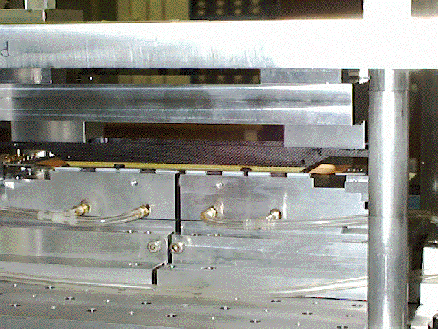
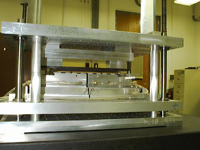
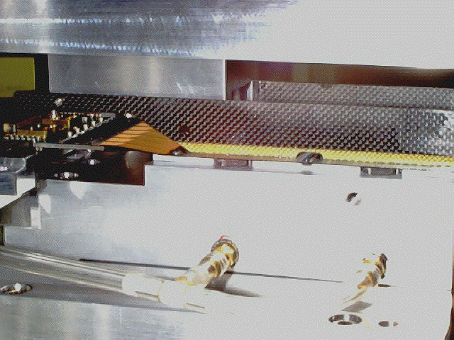
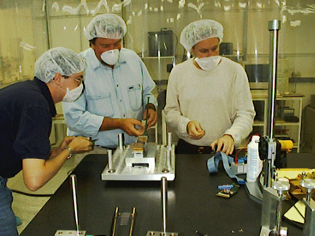
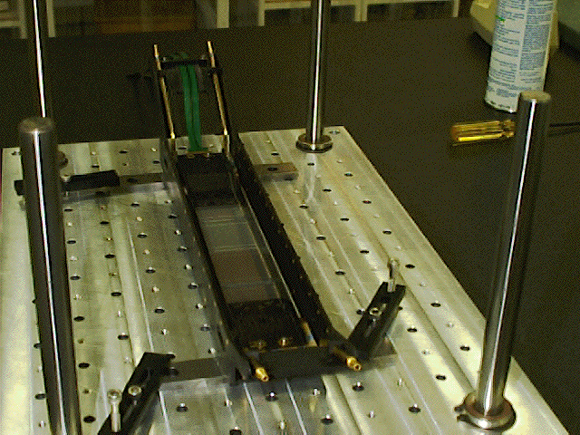
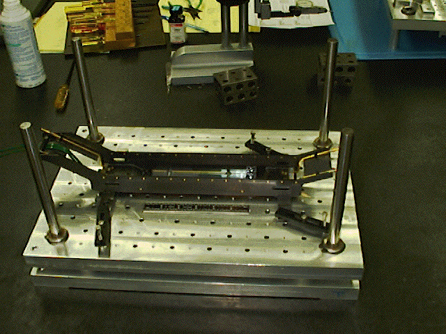
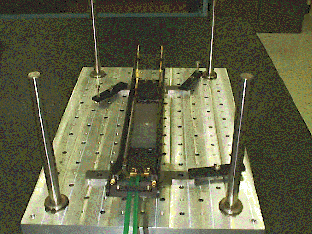
Here are some pictures of the module as the ribs are being glued to the DFAs. The two half modules sit on separate alignment fixtures and are placed on the bottom platen. The rib-endpiece assembly is mounted on a different platen and lowered into place above the half modules. After the epoxy joining the ribs to the silicon has cured, the module is released from the bottom platen, and the top platen is removed, ribs, module and all.
|
|
|
|
|
| Ribs (black carbon fiber with yellow Kevlar at bottom) being attached to the module. | Wide shot of rib attachment fixture. | Close-up of ribs and HDI. | View of the Z-side of the module after the ribs have been glued on. |
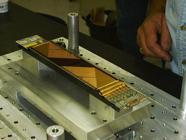
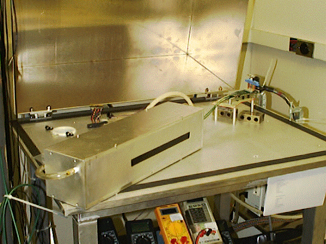
After the ribs were attached, the module was place in a carbon fiber housing. This housing was made at LBNL for use during the commissioning run. It has brass plumbing to bring cool water to the HDI buttons to keep the ICs at a happy temperature.
|
|
|
|
|
| Attaching the tails before placing the module in the CF housing. | Three pictures of the module in the housing... | ||
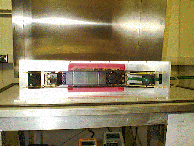
The carbon fiber housing is placed inside a box for use during the beam test. This box provides light tightness and fixturing for water cooling and dry air flow. The box has two thin aluminized mylar windows on either side of the active silicon to reduce the amount of multiple scattering before and after the beam particles pass through the silicon.
|
|
|
|
|
|
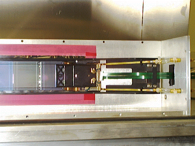
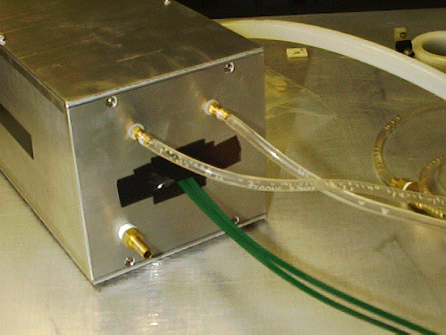
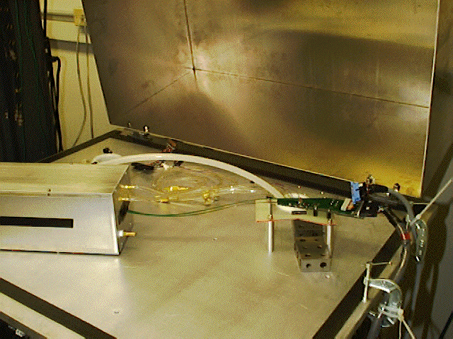
| Picture of the module in the Beam Test Box. The pink tape behind the module is holding an aluminized mylar window in place. | Close-up of the backward half of the module with the 7+7 HDI and cooling system. | End view of Beam Test Box showing the tails (green), water cooling (clear tubes) and dry air outlet (brass fixture). | Connection between box and Matching Card. | Full view of box. |
We have measured gains, intercepts, and noise on every channel before and after bonding. The results are included in the bonding map Excel spreadsheet. A description of the procedure that we used for extracting this information, as well as some typical plots is also available.
Useful information and hints for operation of the module are collected in a separate document. A summary of our experience in struggling with noise problems is also available
We have generated a spreadsheet containing a list of all silicon strip numbers and which IC channel numbers they are bonded to. Bad channels are indicated, as well as the gain and noise. The full spreadsheet is available in Excel format and there is an HTML table just showing the strips flagged with some kind of problem. There is a Microsoft Word document describing the content of the Bonding Map (click here for a browsable version of the document).
![]()
Go To : [Introduction] [Pictures]
[Electronics Measurements] [Operational
hints] [Bonding Map]
Back to the UCSB
BaBar page.
![]()
Any comments or questions? Please send e-mail to Douglas
Roberts ![]()