![]()
![]()
![]() Under Construction
Under Construction
The Light Emitting Diode (LED) DFA Scan test setup was designed as part of the DFA Probe Station for use in electrical testing of detectors during early phases of productrion wirebonding. . The system, which will be refered to as the LED Scan, incorporates; the DFA Probe Station, a precision XY table positioned by stepping motors under the control of a LabVIEW and an LED coupled to optical focusing head via a fibre optic cable assembly.
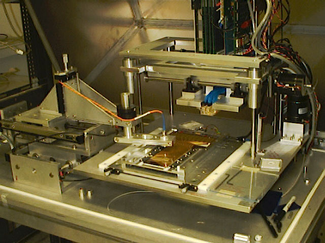
Figure 1. DFA Probe Station shown with optical head positioned over a layer three part.
The LED is a Hewelett Packard part number HP-HFBR-1464T communication quality led, with a wavelength of 820 nm at a power level of -4.5 dbm into a 100/140 um optical cable with100 mA of drive current, the rise and fall times for the part are 3.0 nsec. . The amount of light emitted by the LED was controlled by adjusting the width of the driving pulse between 2 and 3 usec. The pulse is generated by an HP8111A pulse generator which is triggered through a digital interface from a National Instruments gereral purpose interface board as illustrated in the block diagram below. The LED drive amplitude is adjustable over a range from 0 to 5 volts peak.
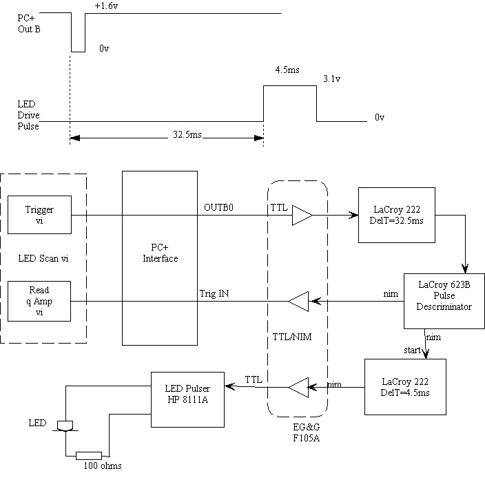
Figure 2. LED Drive Electronics.
The optical head is mounted on an arm at the end of the XY carriage and acts to focus a small spot on the face of the detector under test. A 10 meter length of HP HFBR-AXS010 multimode 100/140 optical fibre interfaces between the LED and the head using ST connectors. The head houses a quarter wave gradient index (GRIN) lens which couples directly to the optical fibre. A 24 mm focal length lens is used to focus a spot on the detector. Measurements show that the smallest spot size that can be achieved is 370 um in diameter.
The XY Table was manufactured by UCSB using VEXTA PH268M stepping motors with 0.9 deg stepping angle. The motors are powered through seperate IM483 Microstepping Drivers which are interfaced to a nuLogic Stepper Motor Conrol Board under LABVIEW control using the nuLogic Motion VI's. The XY table position is established using a pair of SONY Magnescale Model SR108-020 position sensors. With this setup we are able to place the LED spot within +- 5 um of the desired position.
The Detector FAnout Probe Station was developed to carry out production testing DFA's during the wirebonding process. The LED testing features were added to the probe station at the time of the initial design. LED testing was invisioned to be of use in locating breaks in the detector channel surface aluminization since the signal however it turned out that the CsRs measurement was able to take care of this condition. The probe station electronics assembly includes a charge amplifier and associated isolated power supplies which are used in the LED test setup.
The low noise charge amplifier has an input noise level of 1.7 nV per root hz (@ 1khz) with a bandwith of 15 Mhz and a gain of 62 dB. The feedback capacitor was measured at 4.0 pF, giving 0.25 mV/fC, with a 100 megohm shunt giving a decay time constant of 400us. With this capacitance the self noise level is 114 dB below One Minimum Ionizing Level. The amplifier is powered from a + - 15 volt isolated power supply. The input to the 2N6550 JFET is AC coupled. The EL2041 output stage is direct coupled from the input JFET through a cascode stage which reduces the JFET input capacitance and resulting self noise.
Charge amplifier output signals are acquired by the National Instruments PC+ Data Acquisition Board where they are sampled and digitized to a resolution of 14bits.
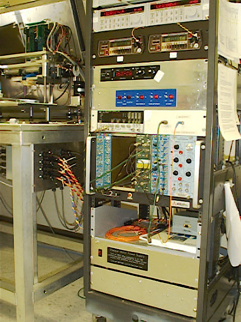
Figure 2. DFA Probe Station Electronics Rack showing LED pulse generator and NIM modules used in data acquisition system.
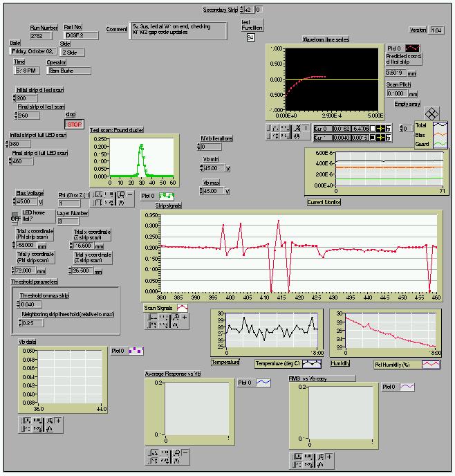
The Virtual Instrument (vi) Main Screen displays the charge amplifier outputs for the selected detector signal strips. The recent charge amplifier output waveform is retained along with time history data related to bias currents and enviornmental data. Test setup information relating to part number, operatior, run number, date-time and neighbor strip configuration are also displayed on the screen. Controls are provided to select bias voltage, initial location parameters of the optical head for the test scan mode and the neighbor strip configuration selection. The screen display is generated as part of the National Instruments LabVIEW software package, the application program is refered to as a virtural instrument.
A series of LED Scan measurements have been carried out on a number of "B" type detectors to study the optical pulse response sutch as; end strip effects, P and N side differences, low capacitance strip response, floating neighbor effects, neighbor fault effects, wafer to wafer differences and charge collection as a function of bulk bias voltage.
A recent study was carried out in an attempt at understanding the end strip effect as evidenced by reduced charge collection by end strips. All data here were taken using the layer 3 DFA D03F-02 which is fully bonded on the phi (n) side and bonded to every other strip on the z (p) side. . . The LED spot was focused on the far end of the z (p) side for each wafer and the far end of W3 for the phi (n) side. . The bias voltage was 45V, and the isolation voltages for the three wafers were W1 @ 40V, W2 @ 24V and W3 @ 22V. The lucite protective covers were removed from the DFA during the measurements. The size of the spot was measured at 3.7 strips at the 70% points representing a spot diameter of 370 micrometeres. A scan was carried out on the Z side of the subject part to study the edge effects, the resulting scan data is shown below. The change from wafer 1 to wafer 2 occurs at relative strip number 47, notice that the end strips outputs for both wafers is 18% below the normal strip average. An analysis follows which models the neighbor strip effects on charge collection.
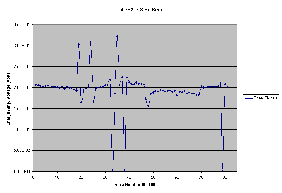
Fault data for the selected detector strips shown in figure 4 are listed in the bad channel list for this detector. In comparing the fault data to the strip output levels the open (plucked) channels are evident (ie. 32,37 & 78) as are the channels which are shorted to floating strip neighbors (ie. 18,23 &34).
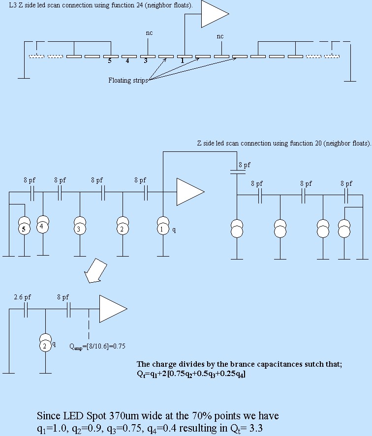
Based on the optical spot size the middle strip will receive one unit of charge (ie. q1=1.0) with the near neighbors receiving 90% and the next neighbors receiving 75%. of the light. When the

Data (run 2782) was collected on D03F.2 at the wafer 1 wafer 2 transition to study the edge effects on carge collection. For the normal Z side strips, the charge collection is q = [210mV/3.3]=63mV and for the strip on the edge of the wafer the charge collection is q = [170mV/2.4]= 72mV. Since the voltage levels only match to within 12% it is suspected that the spot may not be uniform in shape.
Any comments or questions? Please send e-mail to Sam Burke
Last Updated on 12/9/98