This study uses external charge injection from an infrared LED
to address the following questions:
Possible anomalies in the gain of chips exhibiting "Chip 9 / LG"
problems under internal charge injection.
Possible differences in the charge collection efficiency on the
phi side of the inner SVT layers with and without a floating strip.
Possible differences in charge collection efficiency between the phi
(n) and z (p) sides of the inner SVT layers (this is an issue raised by
puzzling results of the 1997 test beam analysis).
Preliminaries
All data here were taken using the layer 1 DFA D01B-6 bonded to
HDI H1-18. The z (p) side of this DFA was fully bonded to AToM
Rad Hard Version 2 chips. Channels for chips 0, 1, and 2 on the
phi (n) side were bonded leaving a floating strip. For the
remaining chips, channels 0-63 were fully bonded, channels 64-127
were bonded leaving a floating strip.
All measurements were performed at 100 nsec shaping time, using a 40
MHZ clock and a 3 microsecond trigger jitter window.
The LED light was shined on chip 3 (phi side) in both the bonded and
1/2 bonded regions, and on chip 9 and 10 (z side). Chip 9 is a chip
which on this HDI exhibits a "Chip 9 / LG" problem; chip 10 is a good
chip. A layer 1 DFA is made up of two separate wafers. In all
measurements presented here light was shined always on the
first wafer. The bias voltage was 37 V, and the isolation voltage
for this wafer is 24 V.
The LED was a HP-HFBR-164T, with a wavelength of 820 nm. The amount
of light emitted by the LED was controlled by adjusting the width
of the driving pulse between 15 and 55 nsec. The risetime of the
LED is of order 5 nsec. The pulse was
generated by a front-panel controlled 50 MHZ HP-8116A pulser, allowing
for good reproducibility of the pulse width. Its amplitude was 2V,
with a 50 Ohm series resistor. Light from the LED
was attenuated by an OD=1 Neutral Density Filter (factor of
10 attenuation). Light also had to pass through a 1/8" lucite
protecting cover, which we did not bother to remove for these
tests (!), and which acted as a convenient mechanical support
for the filter. Light was always shined on the phi side of the detector.
The size of the pulse was of order 600 micron, FWHM.
Methodology
The key ingredient to this kind of measurement is good analog resolution.
We decided not to use the TOT information because we do not feel that
we understand it well enough yet. Therefore, charge collection
measurements were performed using threshold scans, much as in
internal charge injection. This required careful tuning of the
light intensity in order to remain within the limited dynamic range of
the THR DAC.
As it has been recently pointed out,
at the moment our ability to measure offsets is highly
questionable. Therefore, we devised a measurement strategy
that is independent of chip offsets.
The trick is to be able to control the relative amount of
charge deposited by the LED in different runs. This is possible
by varying the width of the LED pulse. Indeed, we appear to
be operating in a region where the deposited LED charge is
linear in the pulse width, see Figure 1.
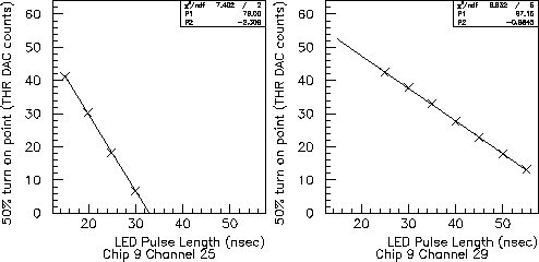
Figure 1: Distribution of 50% threshold turn on point vs the
length of the LED pulse for two channels on the p-side. Note that
thresholds decrease bottom to top, i.e. THR DAC = 0 is the highest
threshold, THR DAC = 63 is the lowest threshold.
Channel 25 is at or near the maximum of the light intensity, channel
29 is further away, hence the difference in slopes.
When operating in the linear region, it can be
shown that
the slopes of fits such as those in
Figure 1 measure the product of channel gain times charge collection
efficiency, weighted by the profile of the LED pulse. Summing up
all of the slopes for all of the channels is equivalent to summing
over the (normalized) LED pulse profile. This sum is therefore
a relative measure of the (average) product of gain and
charge collection efficiency. We will call this quantity eff*g
in the remainder of this document.
Thus our procedure is the following :
For each position of the LED, take 9 threshold scan runs with
LED pulses varying between 15 and 55 nsec in 5 nsec steps.
For each channel, fit the 50% turn on points (in units of THR DAC counts)
as a function of
LED pulse length to a straight line (see for example Figure 1).
Obtain a relative measure of eff*g by summing up the slopes
of all channels.
If so desired, extract the relative charge collection efficiency
eff by correcting for the gain g. This procedure will
be discussed later.
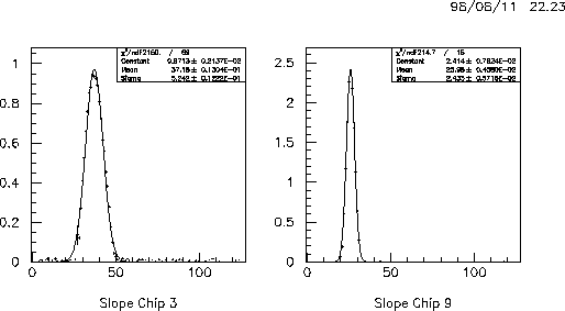
As an illustration, we show in Figure 2 slope distributions as
a function of channel number. Note that the readout pitch
is 50 micron on the phi side and 100 micron on the z side.
From the gaussian fits, the LED spot
on the z side is somewhat wider. This is effect is entirely
due to our focussing system (this was checked by rotating the
lens holder by 90 degrees).
Figure 2:Distribution of slopes as a function
of channel number the phi side (chip 3) and the z side (chip 9) obtained
from a set of 9 runs.
We believe that the main source of uncertainty in our measurents
of eff*g comes from the algorithm chosen to sum up the slopes.
The measurements in the wings of the distributions in Figure 2 are suspect
because they can be affected by noise. In general, we sum the slopes by
fitting to a gaussian and calculating the area under the curve.
Because the distributions are not perfectly gaussians, the answer that
we obtain is affected by the range of the fit. For some reason the
phi side distributions are more affected by this problem, as can
also be seen from careful inspection of Figure 2. Typically we
fit the gaussian for channels that see at least of order 0.5 or
1 fC of charge. The differences in the estimates of the sum of
slopes can be as large as +/- 7% in some cases. When quoting
results below, we will take these effects into account.
In a couple of cases we repeated our measurements
under identical conditions and we reproduced results at the 1%
level or better.
Some Comments on Gains and Noise
The capacitance for phi channels with floating
strips is smaller than without floating strip because
the interstrip capacitance dominates the total capacitance.
Because of this change in capacitance, the noise in the
floating strip configuration is smaller.
It also turns out that the gain of the AToM chip decreases
slightly with capacitance. Using charge injection, we measure
that the gain with a floating strip is approximately 5% higher
than without. In measuring the relative charge
collection efficiencies in the two phi configuration it is
necessary to correct for this effect.
As an aside, the measured reduction in noise in the floating strip
configuration was reported to be approximately 15%. This measurements
neglected to properly account for the change in gain. When this
is done properly, the reduction in noise becomes 20%. It does not
happen very often that
the small factors of a few percent add up in the right direction....
but we'll take them...
Comparison of Floating and Non-Floating Configurations on the Phi Side
This measurement was performed on channels readout by the same chip.
Therefore all systematics due to chip-to-chip process variations
cancel in the comparison. The largest systematic uncertainty
is due to the uncertainty in calculating the sum of slopes.
Using different methods we find the following range of values:
eff*g (float) = (1.07 - 1.20) eff*g (no-float)
eff (float) = (1.00 - 1.14) eff (no-float)
where the relative eff was obtained by correcting the
measured slopes, channel by channel, by the relative gains measured
in internal charge injection. Values for the relative
eff above 1.0 are unphysical. We conclude that our
measurements are consistent with 100% charge collection efficiency
on the floating strips. It is not clear what kind of lower limit
we can place on eff without doing a lot more work.
At this stage we guess-estimate that
eff is greater than something like 0.9.
Chip 9 / LG study
As mentioned above, chip 9 on HDI H1-18 shows symptoms of the
chip 9 / LG problem, whereas chip 10 does not. The systematic
uncertainty in the sum of slopes is now small, because the
LED spot on the two chips has the identical size and shape.
We find the following range of values:
eff*g (Chip 10) = (0.94 - 0.98) eff*g (Chip 9)
This is well within the expected range of chip-to-chip gain variations.
If anything, in this case the Chip 9 / LG chip shows a slightly higher
gain than a neighboring good chip. We conclude that we
do not see any anomaly in the gain of a chip suffering from the
Chip 9 / LG problem.
Comparison of Phi vs Z Charge Collection Efficiency
Here the systematic uncertainty from summing the slopes is
worst because the LED spot is not circular. For example
we find a systematic difference in the phi vs z ratio of
eff*g of 6% when the LED holder is rotated by 90 degrees.
The results shown below remove this effect by averaging the
two sets of measurements, but an uncertainty due to different
summing algorithms remains:
eff*g (phi) = (0.86 - 1.00) eff*g (z)
The measurements are taken on the fully bonded region of chip 3 (phi side)
and on chip 10 (z side). Note that on average we expect the gain
on the z side to be a little larger due to the lower capacitance.
However, the expected chip-to-chip gain variations are probably
just as large.
Finally, we can attempt to factor out the gain in order to
just compare eff using the charge injection data.
However, given the expected chip-to-chip variations in the
charge injection capacitor, it is not clear whether this is a useful
excercise or not. In any case, we find:
eff (phi) = (0.95 - 1.15) eff (z)
We do not see any evidence of a reduced charge collection efficiency
on the z side of a magnitude large enough to explain the
1997 testbeam results.